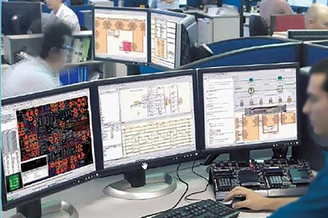
PCB (Printed Circuit Board) engineering is the process of designing and manufacturing printed circuit boards in electronic devices. It involves many different stages and tasks, including design, layout, manufacturing and testing. The following are the main elements covered in PCB engineering:
I. Preparation of Engineering Documents
● Requirements analysis and planning:
Determine the functional and performance requirements of the board.
Determine board size, shape and hierarchy.
Determine the type and number of components.
● Schematic design:
Create a schematic of the circuit using a professional circuit design tool (e.g., Altium Designer, Eagle, KiCad, etc.).
Add components (e.g., resistors, capacitors, integrated circuits, etc.) to the schematic and connect them to achieve the desired function.
● Circuit Simulation:
Use simulation software (e.g. SPICE) to verify the correctness and performance of the circuit design.
Simulation analysis is used to check the behaviour of the circuit under different conditions to ensure that it meets the specifications.
● PCB Layout Design:
Convert the circuit diagram into an actual PCB layout.
Place components and connect them, taking into account signal integrity, power distribution, thermal management, and other factors.
Determine the hierarchy and layer connections.
● Signal Integrity Analysis:
Use tools to perform signal integrity analysis to ensure that high-speed signals are transmitted as required to avoid signal interference and reflections.
● Power Distribution Design:
Determine the layout of power lines to ensure that each component can obtain a stable power supply.
● Hierarchical division:
Determine the hierarchical structure of the PCB, including the design of the inner and outer copper layers.
● Wiring and routing:
Route signal and power lines to minimise interference and maximise performance.
Consider issues such as differential pairs and matching impedance.
● Component library management:
Ensure that the component library contains the required components and that they are used correctly in the design.
● Export to Generate Gerber File:
Prepare Gerber files for PCB fabrication, including information on pads, alignments, drill locations, and more.
II. Manufacturing Preparation:
● Select the PCB board, process and other parameters to meet the design requirements.
Determine the number of layers on the board and decide if holes need to be passed through.
● Production:
Manufacture the PCB board, including processes such as etching, chemical copper plating, jacking, and alignment.
● Assembly:
Soldering components to the PCB, either by hand soldering or automated surface mount technology (SMT).
● Testing and Verification:
Functional testing and performance verification of manufactured PCBs to ensure they meet design requirements.
● Debugging:
Debugging the PCBs as necessary to resolve issues that may arise.
● Documentation:
Ensure that all design documents, manufacturing documents and test records are properly maintained for future reference and production.
Contact: Ella Ouyang
Phone: 86-13570888065
Tel: 86-0755-28632299
Email: ellaouyang@szxpcba.com
Add: Building 8, Gangbei Industrial Zone, Huangtian, Xixiang, Bao’an District, Shenzhen, China.
We chat
